Ficus2 Hardware User Manual
This Hardware Guide provides information about the features, connectors and signals available on the Ficus2 board.
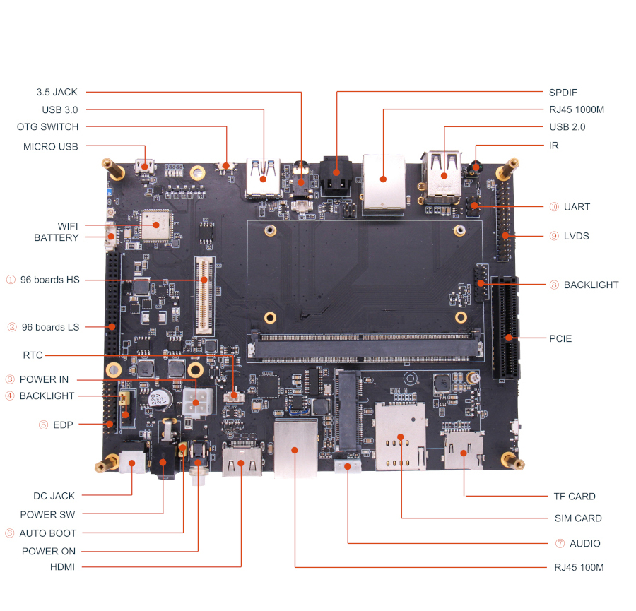
Figure 1.1
1.1 Board Version
Ficus2 board comes with different version. When you get the board, you need to know the hardware version, which is printed in the bottom side of the board.
1.2 Power Supply
The Ficus2 board is powered by a DC 12V supply. There are two solutions for power supply. One with the ATX 12V 4Pin connector. And the other with DC 12V/4V Jack with On/Off switch. But they can not be used at the same time.
As for the current(mA) that the Ficus2 requires, it depends on what is connected to the Ficus2 board.
1.3 Buttons
Power SW is used when the board is power by the DC 12/4V Jack.
USB OTG Switch.
Maskrom Button helps to set the Soc to maskrom mode. Then you could flash system image to eMMC module via USB port.
1.4 LEDs
There are five LEDs on the top-left of the board.
1.5 USB
Ficus2 is equipped with one Micro USB port, one Double Type-A USB 2.0 host port, one Type-A USB3.0 port and so on.
As we know, standard USB categories include high-capacity access, network, Hub, serial converter, audio, video, HID etc. To meed the need mentioned above, here add one USB Hub chip. Therefore the Soc can communicate with so many USB devices.
1.5.1 Micro USB
Ficus2 is equipped with Micro a USB port used for USB serial console, which can access the low level debug message. You can use a Type-A to Micro USB cable with one end connected to the PC and the other end connected to the Micro USB port on board.
On PC, like Windows, Linux or Mac, you can use some software that is already built for serial console. For example, Putty, Minicom and so on.
1.5.2 Double Type-A USB 2.0 host port
As mentioned above, there is one USB Hub chip includeing a USB 2.0 high speed 4-port Hub controller on board. Two lanes that chip provides are for this Double Type-A USB 2.0 host port.
This port enables the attachment of peripherals such U Disk, keyboards, mice, USB dongle etc.
1.5.3 Type-A USB 3.0 port
There is one USB OTG switch near the USB 3.0 port.
When the USB OTG switch is switched to the host side, the Type-A USB 3.0 port also enables the attachment of peripherals such U Disk, keyboards, mice, USB dongle etc.
Compared with USB 2.0 host port, this USB 3.0 port supports On-The-Go(OTG) when the USB OTG switch is switched to the device side. Thus the Soc is recognized as an device.
Take adb as an example. You can use a Type-A to Type-A cable as a bridge between you PC and Ficus2 board. In addition to the Ficus2 system configuration, you can setup the adb tool on your PC to access Ficus2 over adb.
1.5.4 The other USB lanes
The USB Hub chip provides four USB lanes. Besides two lanes used for Double Type-A USB 2.0 port, another USB lane meets the need of the communication between Soc and 4G module.
The other lane is layout to the low speed connector.
1.6 Ethernet and PoE(Power Over Ethernet)
The Ficus2 is equipped with two Ethernet sockets. One is GbE with PoE support and the other is 10/100Mbit Ethernet.
Remember that there are Gigabit Ethernet cable and 100Mbit Ethernet cable.
1.7 WiFi and Bluetooth
The wireless module AP6256 is on board. It supports 802.11 ac wifi with 2.4G&5G Hz RF and Bluetooth 5.0. For better performance, on board anterna is equipped. Besides, an uFL antenna socket is reserved.
1.8 Mini PCIe 4G Module with SIM card
From our test, 4G module like Quectel EC20 and SIM card are available on Ficus2 board.
This module communicates with Soc like RK3399Pro over USB.
1.9 Audio
On Ficus2 board, audio can be played through speakers or headphones using a standard 3.5mm jack.
The definition of Speaker connector marked with number 7 in figure 5.1 is shown below.
| Pin# | Name |
|---|---|
| 1 | HPL_VOP |
| 2 | HPL_VON |
| 3 | HPR_VOP |
| 4 | HPR_VON |
1.10 HDMI
Any HDMI monitor should work as a display for the Ficus2 board ad the HDMI interface is following the standard.
HDMI CEC is supported.
The HDMI interface pin specification shows below.
| Pin# | Name |
|---|---|
| 1 | HDMI_TX2P |
| 2 | GND |
| 3 | HDMI_TX2N |
| 4 | HDMI_TX1P |
| 5 | GND |
| 6 | HDMI_TX1N |
| 7 | HDMI_TX0P |
| 8 | GND |
| 9 | HDMI_TX0N |
| 10 | HDMI_TXCP |
| 11 | GND |
| 12 | HDMI_TXCN |
| 13 | PORT_CEC |
| 14 | NC |
| 15 | DDC_SCL |
| 16 | DDC_SDA |
| 17 | GND |
| 18 | VCC5V0_HDMI |
| 19 | HDMI_HPD |
1.11 IR receiver
IRM-3638 module is equipped. its carrier frequency is 38 KHz. And the date rate is high, up to 4000 bit/sec.
1.12 RTC
The RTC battery connector is designed using the standard connector type.
| Pin# | Name |
|---|---|
| 1 | GND |
| 2 | +3.3V |
1.13 S/PDIF Socket
S/PDIF socket is equipped for digital audio output.
1.14 SPI Nor Flash
One SPI Nor Flash is on board. Its power supply voltage is 1.8V.
1.15 LVDS Connector
There are eight lanes LVDS included in LVDS connector.
The definition table of the LVDS connector is this.
| Pin# | Name | Pin# | Name |
|---|---|---|---|
| 1 | VDD | 2 | VDD |
| 3 | VDD | 4 | GND |
| 5 | GND | 6 | GND |
| 7 | LVDS_D0N | 8 | LVDS_D0P |
| 9 | LVDS_D1N | 10 | LVDS_D1P |
| 11 | LVDS_D2N | 12 | LVDS_D2P |
| 13 | GND | 14 | GND |
| 15 | LVDS_CLK0N | 16 | LVDS_CLK0P |
| 17 | LVDS_D3N | 18 | LVDS_D3P |
| 19 | LVDS_D5N | 20 | LVDS_D5P |
| 21 | LVDS_D6N | 22 | LVDS_D6P |
| 23 | LVDS_D7N | 24 | LVDS_D7P |
| 25 | GND | 26 | GND |
| 27 | LVDS_CLK1N | 28 | LVDS_CLK1P |
| 29 | LVDS_D8N | 30 | LVDS_D8P |
1.16 eDP Connector
eDP is the display interface. The definition table of the eDP connector is shown below.
As you can see, four lanes are layout.
| Pin# | Name | Pin# | Name |
|---|---|---|---|
| 1 | EDP_TX0P | 2 | EDP_TX0N |
| 3 | GND | 4 | GND |
| 5 | EDP_TX1P | 6 | EDP_TX1N |
| 7 | GND | 8 | GND |
| 9 | EDP_TX2P | 10 | EDP_TX2N |
| 11 | GND | 12 | GND |
| 13 | EDP_TX3P | 14 | EDP_TX3N |
| 15 | GND | 16 | GND |
| 17 | EDP_AUXP | 18 | EDP_AUXN |
| 19 | VDD | 20 | GND |
1.17 PCIE X4 Socket
PCIE X4 Socket is designed with the standard of NGFF.
It is suitable for something like NVME M.2 NGFF PCIe x4 SSD Card etc.
1.18 96boards standard 40P Low Speed Connector
The following table shows the signals on the2 x20 female 2mm connector.
Empty cells are not connected(NC) pins.
| Pin# | Name | Pin# | Name |
|---|---|---|---|
| 1 | GND | 2 | GND |
| 3 | CTSA_1V8 | 4 | PWRON |
| 5 | TXA_1V8 | 6 | RESET_L |
| 7 | RXA_1V8 | 8 | SPI1_CLK |
| 9 | RTSA_1V8 | 10 | SPI1_RXD |
| 11 | TXB_1V8 | 12 | SPI1_CS0 |
| 13 | RXB_1V8 | 14 | SPI1_TXD |
| 15 | I2C1_SCL | 16 | I2S0_LRCK_RX |
| 17 | I2C1_SDA | 18 | I2S0_SCLK |
| 19 | I2C6_SCL | 20 | I2S0_SDO0 |
| 21 | I2C6_SDA | 22 | I2S0_DSI0 |
| 23 | PWM3 | 24 | I2S_CLK |
| 25 | GPIO3_D4/I2S0_SDI1 | 26 | I2C8_SCL |
| 27 | GPIO3_D5/I2S0_SDI2 | 28 | I2C8_SDA |
| 29 | GPIO3_D6/I2S0_SDI3 | 30 | I2C4_SCL |
| 31 | CAM_RST0 | 32 | I2C4_SDA |
| 33 | CAM_RST1 | 34 | CAM_PWR0 |
| 35 | VCC_1V8 | 36 | VCC12V_DCIN |
| 37 | VCC5V0_USB | 38 | VCC12V_DCIN |
| 39 | GND | 40 | GND |
The low speed connector provides
- UART x2
- SPI x1
- I2S x1
- I2C x4
- GPIO x12
- PWM x1
1.19 96boards standard 60P High Speed Expansion Connector
The following table shows the signals on the 0.8mm 50 ohm high speed receptacle.
Empty cells are not connected(NC) pins.
| Pin# | Name | Pin# | Name |
|---|---|---|---|
| 1 | SPI1_TXD | 2 | MIPI_TX1/RX1_CLKP |
| 3 | 4 | MIPI_TX1/RX1_CLKN | |
| 5 | 6 | GND | |
| 7 | CAM_PWR1 | 8 | MIPI_TX1/RX1_D0P |
| 9 | SPI1_CLK | 10 | MIPI_TX1/RX1_D0N |
| 11 | SPI1_RXD | 12 | GND |
| 13 | GND | 14 | MIPI_TX1/RX1_D1P |
| 15 | MCLK_OUT | 16 | MIPI_TX1/RX1_D1N |
| 17 | MCLK_OUT | 18 | GND |
| 19 | GND | 20 | MIPI_TX1/RX1_D2P |
| 21 | MIPI_TX0_CLKP | 22 | MIPI_TX1/RX1_D2N |
| 23 | MIPI_TX0_CLKN | 24 | GND |
| 25 | GND | 26 | MIPI_TX1/RX1_D3P |
| 27 | MIPI_TX0_D0P | 28 | MIPI_TX1/RX1_D3N |
| 29 | MIPI_TX0_D0N | 30 | GND |
| 31 | GND | 32 | I2C2_SCL |
| 33 | MIPI_TX0_D1P | 34 | I2C2_SDA |
| 35 | MIPI_TX0_D1N | 36 | I2C7_CLK/GPIO2_B0 |
| 37 | GND | 38 | I2C7_SDA/LID# |
| 39 | MIPI_TX0_D2P | 40 | GND |
| 41 | MIPI_TX0_D2N | 42 | MIPI_RX0_D0P |
| 43 | GND | 44 | MIPI_RX0_D0N |
| 45 | MIPI_TX0_D3P | 46 | GND |
| 47 | MIPI_TX0_D3N | 48 | MIPI_RX0_D1P |
| 49 | GND | 50 | MIPI_RX0_D1N |
| 51 | DP4 | 52 | GND |
| 53 | DM4 | 54 | MIPI_RX0_CLKP |
| 55 | GND | 56 | MIPI_RX0_CLKN |
| 57 | 58 | GND | |
| 59 | 60 | Reserved |
The high speed expansion connector provides
- MIPI CSI x2 (4 lanes + 2 lanes)
- MIPI DSI x1 (4 lanes)
- USB HOST x1
- I2C x2
Pin#60 is connected to +1V8 power supply through a 10K resistor.
1.20 UART Connector
The following table shows the signals on the UART connector.
| Pin# | Name | PIn# | Name |
|---|---|---|---|
| 1 | NPU_UART2_RX | 2 | NPU_UART2_TX |
| 3 | XR_TXD | 4 | XR_RXD |
| 5 | UART2_RX | 6 | UART2_TX |
Connection for CPU debug console

Connection for NPU debug console

1.21 Backlight Connector (Marked with number 4 in figure 1.1)
The following table shows the signal.
| Pin# | Name |
|---|---|
| 1 | VDD_LCD |
| 2 | VCC3V3_SYS |
| 3 | VDD_LCD |
| 4 | VCC5V0_USB |
| 5 | VDD_LCD |
| 6 | VCC12V_DCIN |
1.22 Backlight Connector (Marked with number 8 in figure 1.1)
The following table shows the signal.
| Pin# | Name |
|---|---|
| 1 | VCC12V_DCIN |
| 2 | VCC12V_DCIN |
| 3 | BL_EN1 |
| 4 | BL_ADJ1 |
| 5 | GND |
| 6 | GND |
1.23 Core Board Socket
More details see VMARC RK3399Pro SOM and VMARC RK3399Pro SOM boards.